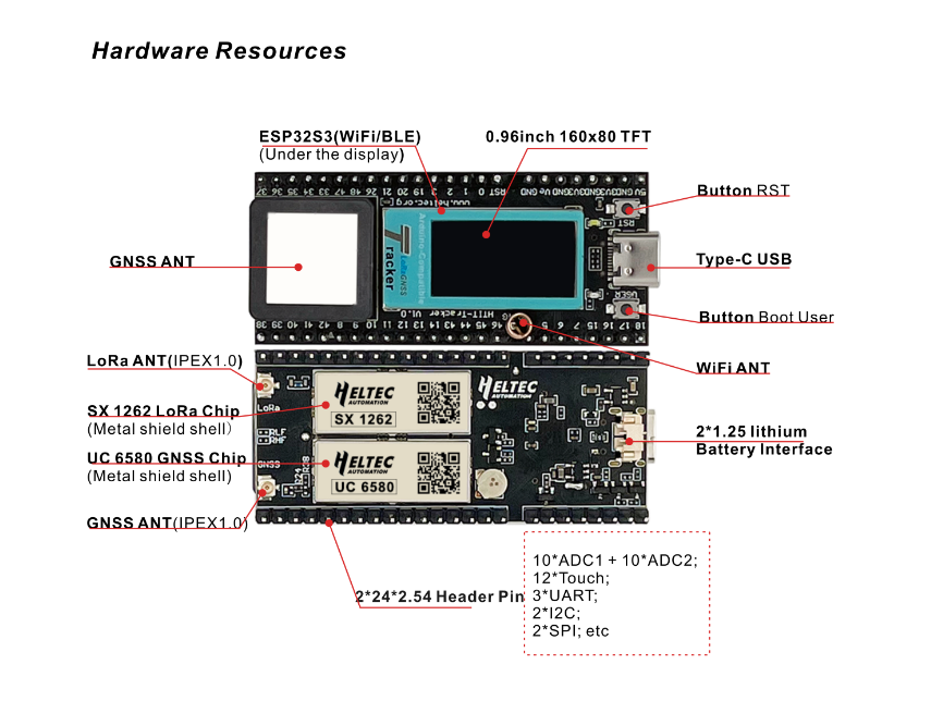
This page provides a reference to the key components and circuit blocks in the Wireless Tracker. For full schematics, see the Downloads page.
The power section provides battery charging, voltage regulation, and power path management.
| Component | Value/Part | Function |
|---|
| F1 | 6V 500mA | Input fuse |
| D1 | RSB6.8S | TVS diode (ESD protection) |
| D2 | 1N5819 | Schottky diode (reverse polarity) |
| Q1 | AO3401 | P-channel MOSFET (power switch) |
| U2 | TP4054 | Li-Po charger IC |
| U4 | CE6260B33M | 3.3V LDO (main) |
| U6 | CE6260B33M | 3.3V LDO (Vext) |
| R16 | 2K/5% | Charge current programming |
| Component | Value | Function |
|---|
| R13 | 390K/1% | Voltage divider (high side) |
| R14 | 100K/1% | Voltage divider (low side) |
| Q3 | S9013 | ADC enable transistor |
Voltage divider ratio: 4.9:1 → VBAT = ADC × 4.9
The main MCU handles all processing, connectivity, and peripheral control.
| Component | Value | Function |
|---|
| U5 | 40 MHz | Main crystal |
| C19, C20 | 22pF | Main crystal load caps |
| X1 | 32.768 kHz | RTC crystal |
| C8, C22 | 4.7pF | RTC crystal load caps |
| GPIO | Function | Notes |
|---|
| 0 | USER_Key | Boot select / user button |
| 1 | Vbat_Read | Battery ADC input |
| 2 | ADC_Ctrl | ADC enable control |
| 3 | Vext_Ctrl | External power control (V1.1) |
| 8-14 | LoRa SPI | NSS, SCK, MOSI, MISO, RST, BUSY, DIO1 |
| 18 | LED | User LED control |
| 19/20 | USB | D-/D+ native USB |
| 21 | LED_K | TFT backlight |
| 33-36 | GNSS | TX, RX, RST, PPS |
| 38-42 | TFT | CS, RES, RS, SCLK, SDIN |
The LoRa transceiver provides long-range, low-power wireless communication.
| Component | Value | Function |
|---|
| L1 | 2.7nH | RF matching |
| L2 | 24nH | RF filter |
| L3 | 2.0nH | RF matching |
| C12, C15, C18, C25 | 0.1µF | Decoupling |
| C13, C14 | 1.8pF | RF matching |
| U11 | UPG2179 | RF switch |
| X4 | 32 MHz | TCXO |
| E4 | IPEX | LoRa antenna connector |
| Signal | GPIO | Direction |
|---|
| NSS | 8 | Output (chip select) |
| SCK | 9 | Output (clock) |
| MOSI | 10 | Output (data to SX1262) |
| MISO | 11 | Input (data from SX1262) |
| RST | 12 | Output (reset) |
| BUSY | 13 | Input (busy indicator) |
| DIO1 | 14 | Input (interrupt) |
The GNSS receiver provides multi-constellation positioning with L1+L5 frequencies.
| Component | Value | Function |
|---|
| X2 | 26 MHz | Main TCXO |
| X3 | 32.768 kHz | RTC crystal |
| C34, C41 | 4.7pF | Crystal load caps |
| R27 | 10K | Reset pullup |
| Component | Value | Function |
|---|
| U8 | HDDL1L5RSS-B8 | L1/L5 LNA |
| U10 | SW7125DE | RF amplifier |
| E3 | IPEX | GNSS antenna connector |
| Component | Value |
|---|
| L4 | 68nH |
| L5 | 1nH |
| L6 | 2.2nH |
| L7 | 18nH |
| L9 | 6.8nH |
| L10 | 7nH |
| L11 | 4.5nH |
| EL2 | 1µH |
| Signal | GPIO | Direction |
|---|
| TX | 33 | GNSS → ESP32 |
| RX | 34 | ESP32 → GNSS |
| RST | 35 | Reset (active low) |
| PPS | 36 | 1PPS timing pulse |
The 0.96” TFT display (ST7735S driver) provides visual feedback.
| Signal | GPIO | Function |
|---|
| SDIN | 42 | SPI data |
| SCLK | 41 | SPI clock |
| RS (DC) | 40 | Data/Command select |
| RES | 39 | Reset |
| CS | 38 | Chip select |
| LED_K | 21 | Backlight (via Q4) |
| Pin | Signal | Notes |
|---|
| VBUS | VDD_5V | 5V power input |
| DN1/DN2 | USB_N | Data negative |
| DP1/DP2 | USB_P | Data positive |
| CC1 | R3 (5.1K) | Configuration channel |
| CC2 | R6 (5.1K) | Configuration channel |
| LED | Color | Resistor | Function |
|---|
| LED1 | Orange | R7 (330Ω) | Charging indicator |
| LED2 | White | R10 (330Ω) | User LED (GPIO18) |
| Button | Function | GPIO |
|---|
| S1 | RESET_SW | RST |
| S2 | USER_SW | GPIO0 |